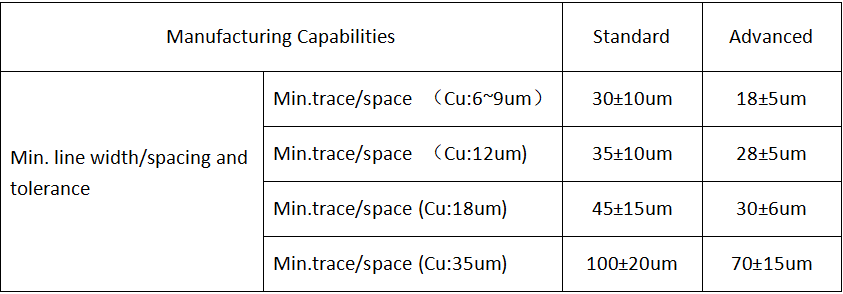
A: For ultra-precision products, we can reach 18±5um. Customized designs are available based on customers’ drawings. Kindly refer to the table below detailing our precise manufacturing process capabilities.
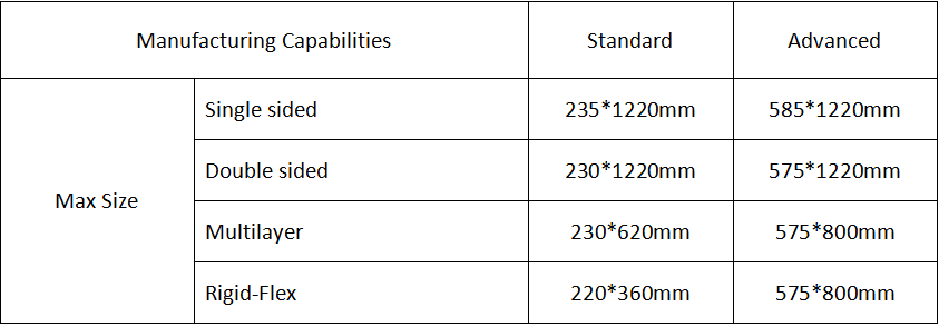
A: The maximum size we can achieve is 585×1220 mm, subject to product stack-up details. Please refer to the table below for detail info.
A: Yes, we can control the impedance tolerance at +/-10%. Under special conditions, the tolerance can be controlled within ±7.5%. Measurement is carried out using a TDR impedance tester.
A: We can only quote FPC prices after receiving corresponding design information.
A: Our monthly production capacity is 20,000㎡.
A: Our fastest turnaround from engineering file preparation to sample delivery is one week.
A: At present, the highest structure we can achieve is 2+N+2 stacked blind vias, with a minimum blind via diameter of 50 μm.
A: We can recommend proper stack-up design and impedance trace width & spacing based on target board thickness and impedance requirements.We can also suggest suitable copper thickness and trace width according to current-carrying capacity specifications.
A: We offer one-stop services from bare boards to FPC assembly, including SMT reflow soldering and selective wave soldering. For FPCA, we conduct test coverage analysis and support ICT testing, FCT testing as well as MCU testing.
A: Yes, we can control the impedance tolerance at +/-10%. Under special conditions, the tolerance can be controlled within ±7.5%. Measurement is carried out using a TDR impedance tester.
A: Yes. Our products are widely used in smart glasses, digital camera lens barrels, medical devices, dexterous hands, robotic arms, hard disk read-write heads, etc. We have rich experience in projects requiring flex cycles ranging from 100,000 times to several millions, even over ten million cycles.
A: Yes. We have obtained UL certifications for single-layer FPC, double-layer FPC, multi-layer FPC, rigid-flex boards and double-layer rigid PCBs.